

Mass Effect: The Intertwined Future of CCD and TDI
CMOS and CCD still matter at the ragged edges of line scan performance. But soon, the conversation may change even for TDI.
For most area and line scan imagers, CCDs are indeed history. But at the high end, where pristine imaging is required under low light, CCD continues to deliver what today’s CMOS imagers simply cannot deliver yet. That’s going to change.
Very often, change in one industry will shape the future of another. Mobile phone camera makers moved their cameras, the world’s highest volume imager application, to CMOS sensors and remapped the global economics of digital imaging. This had direct implications for the machine vision industry, as area and line scan imagers rode this influx of investment to displace CCDs as the go-to imager of choice.
Even as CMOS has caught up with CCD in performance for more common applications, the differences between their designs mean they are not equal in the most demanding ones. Hence the time-honored debate: CMOS or CCD? Such an easy to understand dichotomy just couldn’t last. It looks like CMOS will take over in most cases, but there remains a complicating exception: TDI.
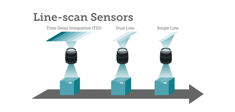
So What is TDI Good For?
As with technology in machine vision, the sensor technology has to match the job [PDF]. TDI sensors are useful in situations where light levels are low, creating a requirement for long exposures. By timing the transfers to occur at the same rate that the image moves across the arrays, each array captures the same image segment.
Adding the data together essentially turns the TDI array into a line array with an effective exposure time equal to the sum of the exposure times for each line. Using a TDI array in this manner, for example, allows line scan imaging where high-speed motion would result in too short an exposure for a single line sensor. This makes TDI imaging most useful when signals are very weak—typically scientific research, medical, aerial reconnaissance, earth imaging, and other high-performance applications.
The Right Scan for the Job
By looking first at their application needs, developers can avoid getting mired in trying to evaluate the complex and subtle differences between CCD and CMOS image sensor technologies. Having insight into the attributes that are significant to their project and knowing the relative importance of those attributes can go a long way toward making the right technology selection.
While the read noise in a single CMOS sensor is quite a bit lower than a comparable CCD solution, the architectural differences between the two increase dramatically as the number of scan lines go up. Because CCD sensors add pixel data together without added noise, they achieve an N-fold increase in signal-to-noise ratio with N lines. In contrast, a conventional CMOS sensor cannot sum pixel data without increasing the noise level with each addition.
So a simple 100-line CMOS sensor would add 100 times the read noise, while the CCD TDI sensor that only needs to read once would only add one read noise component. In linescan applications that only involve a few lines, CMOS will still have an advantage, because the read noise in a modern CMOS sensor is quite a bit than a CCD solution. But once in the realm of hundreds of lines in TDI applications, CCD still has the advantage. This TDI Calculation Worksheet can help you see how this might apply to your application.
In the end, the low-noise performance of a multi-stage CCD TDI sensor makes it the ideal choice for inspection systems that focus on high-quality images under low light conditions.
Everything Changes: Technologies, Approaches, and Your Choices
The world is changing. Going forward, it may be best to simply forget about CCD vs. CMOS. The first step is to determine whether you require TDI operation—meaning that your application is too light-starved for vanilla line scan. If the answer is “yes,” then you’ll need to recognize that there are two ways to achieve TDI functionality: charge domain and voltage domain.
If you are committed to a CCD process, then your choice is simpler. The only practical way to build a CCD TDI is with a charge domain architecture. But, if you have a CMOS process at your disposal, you may have more options. To date with CMOS, you have been pretty much restricted to building voltage domain TDI devices.
But lately, people have begun to modify CMOS processes so that charge domain TDI devices can be built. By integrating charge domain TDI pixels on a CMOS process, IMEC and others have developed chip technologies that combines the best of both worlds. The CMOS technology enables on-chip readout, operating at higher speeds, lower noise and lower power consumption that’s not possible with traditional CCD technology. This promises the best of both worlds – the combined the ability to scale to any number of rows as with a CCD, but take advantage of the lower readout noise of CMOS. That could give us the equivalent of one-stop shopping for most applications.
Until charge domain CMOS solutions become mature (they aren’t yet), charge domain (and therefore CCD) has superior SNR when a large number of stages is needed (greater than 24). Voltage domain CMOS will achieve better SNR over a small number of stages. It’s probably best to talk to a company that does both…
 Five CMOS Camera Developments to Watch in 2014
  Industrial Inspection: Line-scan-based vision system tackles color print inspection