

CMOS TDI: A Game Changer in High-Fidelity Imaging
After years of development, CMOS Time Delay & Integration is having an impact on satellites, in medical imaging and everywhere in between.
Technology often moves forward in secret. It typically delivers incremental improvements to the insiders in the industries it already calls home. But, once in a while, it achieves a breakthrough point…and whole societies can change as a result. Often this happens in the consumer space, where big budgets and large consumer bases can transform toys into productivity tools for huge portions of the world—in cars, computers, and phones.
But sometimes it breaks from one industry into many, without catching the notice of consumer-focused media and industries. Today, as a result of high-speed machine vision, more of our food is inspected than ever before. We know more about our planet’s history and climate due to higher resolution and new modalities of imaging from satellites. On April 24, 2018, California police were able to lay murder charges against a suspect they had been chasing for the last four decades, and were only able to identify him through DNA evidence from consumer heritage websites, which is only possible, affordable, and widely available because TDI (Time Delay and Integration) imaging has become so good.
TDI has always been dedicated to high-end, low-light, high-performance applications, and as technology has shifted from CCD to CMOS imaging, TDI as an approach to solving challenging imaging problems is expanding up, down, and out. So much so that today we can imagine solutions for problems that were impossible even a few years ago.
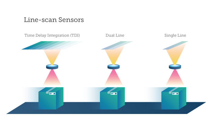
Time Delay and Integration Imagers
Just four years ago, it seemed that CMOS sensors were not quite ready for TDI imaging, which is used to increase the signal-to-noise ratio (SNR) when imaging fast moving objects in low light. In line scan imaging, TDI captures tens of hundreds of lines. Each line successively captures a snapshot of the object as it passes, allowing the accumulation of multiple images that can result in a very low noise image of a dark or hard-to-image object. As a result, TDI is used in everything from web inspection to satellite-based imaging: anywhere where speed is high and light is low. Combined with CMOS sensor design innovations like back-side-illumination, sophisticated CMOS TDI cameras are bringing new possibilities to space applications.
In the Beginning…
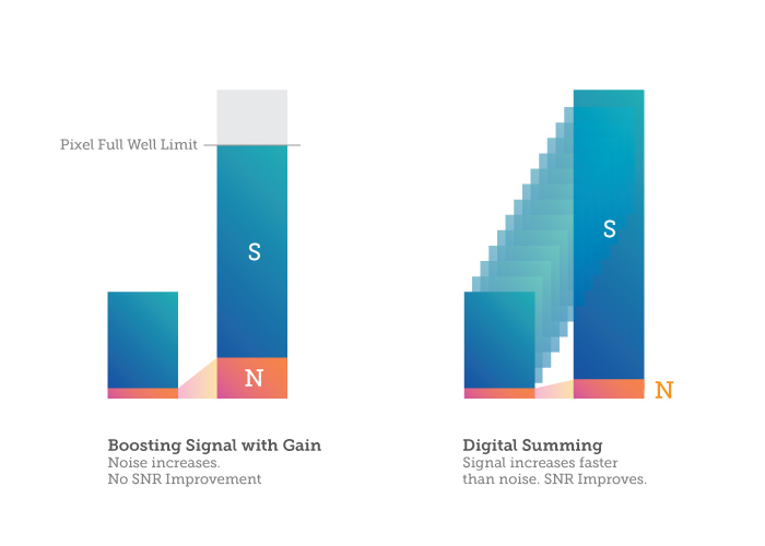
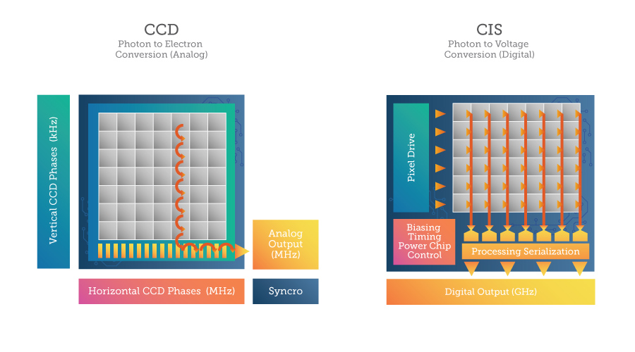
In CCDs, the signal summing operation across pixels is noiseless but this is not the case with CMOS: the former combine signal charges while the latter combines voltage signals. This made for some very noisy CMOS TDI imaging in the beginning, because the noise was increasing with the number of lines, much more noise than you’d get with a standard CCD solution, and even if you were using the most sophisticated CMOS sensor you could get your hands on. With the introduction of a few new technologies, that’s changed.
Reshaping the High End
While CMOS continues to take the lead in terms of size, power, ease of integration, frame rate, and manufacturing cost, CCD still rules when it comes to noise and efficiency. This sticking point took on new urgency in 2015, when Sony announced its plans to end large-scale production of CCD sensors. The popularity of CCD was falling: commenting on the Sony news, Stemmer Imaging shared that the share of CMOS sensors sales vs. CCD had almost tripled from 2010-2014, and they expected it to keep rising.
That same year, a few companies released their first serious attempts at a CMOS-based TDI cameras. After years of development, Teledyne Dalsa announced the Piranha XL, which comes as a 16k, 12-stage, 125kHz TDI camera. When combined with an equally high performing frame grabber, the Piranha XL could achieve performance and low noise that wasn’t possible before with CMOS with the help of “digital summing,” a processing approach that only increased noise by the square-root of the number of stages, enabling stronger signal and less noise even with many TDI stages. While high-speed CCD imagers have a large number of parallel fast output channels, each pixel does not have its own amplifier, resulting in higher relative bandwidth for a CCD amplifier compared to a CMOS amplifier, resulting in higher noise within the image. Consequently, high-speed CMOS imagers can be designed to have much lower noise than high-speed CCDs.
“This combination has exceeded performance expectations for light-starved applications where sensitivity, resolution and high-speed image capture and transfer are critical.”
– Eric Fox, Director, Business Development at Teledyne DALSA
Hybrid CCD-in-CMOS Sensors
Lately, companies and individuals are focused on how to modify CMOS processes so that charge domain TDI devices can be built. By integrating charge-domain TDI pixels on a CMOS process, companies like IMEC, ViewWorks, e2v, and others have been developing sensor technologies that combine the best of both worlds.
Another approach was to mimic the low-noise architecture of CCD within a CMOS sensor. CCD-like pixels would be able to sum charges without noise but still be produced on a CMOS process. This unique approach promised the best of two worlds: the noiseless collection and transfer in charge domain of the CCD technology, and the system integration potential that includes low power and fast readout. Contrary to traditional imagers that read out pixels per column and multiplex the data to one analog-to-digital convertor (ADC), the new imager uses one ADC per column, and the different columns are read out in parallel. CMOS also allows a dedicated output amplifier per column, allowing fewer charge transfers and higher line rates. The CMOS process also allows lower power consumption, smaller pixels, and extra on-chip functionality which can simplify overall system design.
Called a “charge-domain CMOS TDI,” this approach takes considerable investment to develop, fine tune, and perfect. Mobile phones and consumer cameras require neither TDI nor charge summing, so there was no coattail of technology investment for this approach to ride on.
For the highest performance applications, the investment is well worth it. Teledyne DALSA’s Linea HS camera, which uses charge-domain CMOS TDI, delivers triple the line rate of CCD TDI with similar sensitivity. The switch also takes advantage of other innate advantages of CMOS. CMOS fabrication techniques allow the individual rows to be located on a single die and much closer together due to CMOS chip architecture, yielding several benefits. The closer the sensor rows, the less time needed to pass between exposures in a multi-line CMOS line scan camera. This means vibrations common to industrial environments and high-speed machinery don’t affect image-acquisition, as the exposures are taken so quickly and close together that vibration doesn’t have time to impact the camera’s FOV.
EMCMOS: Supercharging the Sensor
While they’ve come very far, the sensitivity of CMOS image sensors remains limited by the readout noise that occurs when used for extremely low light applications (in terms of microluxes). To this end, the scientific market has turned to electron multiplying CCD (EMCCD), which operates with electronic multiplication and can therefore potentially reduce noise levels.
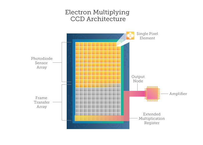
The main principle of electron multiplication is to apply a gain to the signal prior to the addition of any noise that occurs as a result of the readout chain. In this manner, the noise is divided by this gain to ultimately improve the SNR. As a result of the CCD principle, the signal is then transferred in the form of electron packets, during which the multiplication is applied to each pixel prior to reading out.
Since CCDs are being replaced by CMOS in nearly every application, it makes sense that people are experimenting with the equivalent EMCMOS. For CMOS applications, the signal is in the voltage domain thereby signifying that the multiplication must be applied prior to transferring the floating node and before adding the noise from the source follower transistor. This technology can improve image quality for both scientific or surveillance applications since it effectively eliminates read noise from an image sensor. This enables advanced ultra-low light applications that require extreme sensitivity at fast frame rates such as adaptive optics and ‘lucky imaging.’ Teledyne e2v combines this approach with its own back-thinning technology and anti-reflection coatings to deliver the quantum efficiency needed for ground-and-space-based astronomy applications.
Keeping up with the CMOS(es)
The current state of play for CMOS in terms of speed and resolution means large amounts of data. For example, Teledyne e2v’s Lince 11M camera produces 4k images at 610fps. Sensors are accelerating past other parts of the data pipeline, and for the foreseeable future, dealing with this data is going to have to be a ‘brute force’ approach to processing.
When you add the image quality and multiple stages of TDI you end up dealing with a staggering amount of data. Teledyne DALSA’s recently released Linea HS TDI camera delivers up to 16K imaging over 192 lines with a max line rate of 300kHz. This kind of high speed and sensitivity is ideal for demanding applications such as flat panel display inspection, wafer inspection, printed circuit board inspection, and high-performance document scanning.
But how are the rest of systems going to keep up?
To harness the power of these new cameras, integrators will turn to CLHS and CXP12, new standards being shaped by the capabilities of these new cameras. The next-generation CLHS interface with deliver up to 8.4 Gbps over a single fiber optic cable (with error correction), which will convey additional advantages. CXP12 will deliver 1.2 GBytes per second, with up to 4.8Gbytes/sec when four cables are used simultaneously.
Another approach will be 3D sensor design to achieve more compact design and faster interconnects. By literally stacking memory, CPUs, and other key components under the camera, the data has a very short distance to travel, enabling faster transfer.
Putting CMOS TDI Data into Play: DNA Sequencing
It wasn’t just one murderer that police have successfully found with DNA evidence. It’s a method that is becoming more and more effective at solving previously impossible cases. The technologies behind this will soon be generating petabytes of genomic information every year. DNA analysis and sequencing can be used for the observation, identification, and characterization biological systems, helping with pathogen detection, disease screening, biohazard detection, cancer diagnostics, and genetic research.
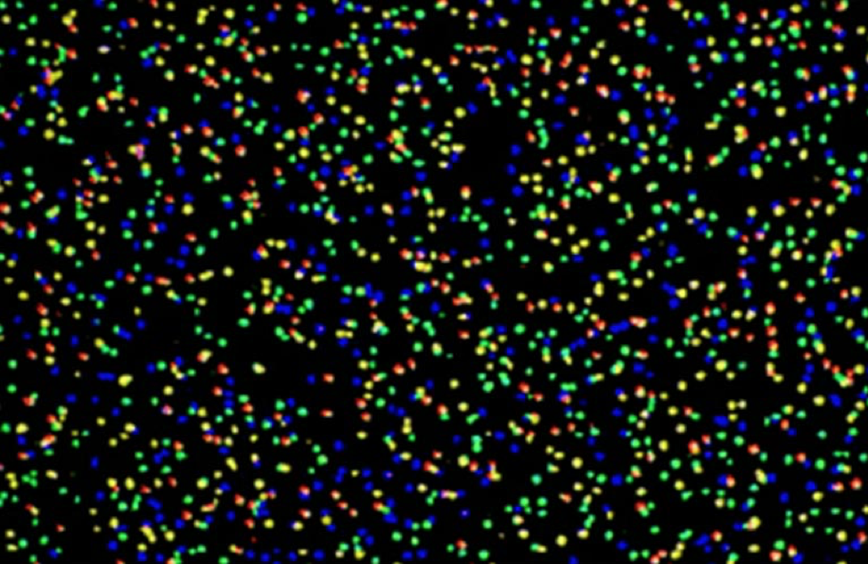
DNA sequencers automatically decode base sequences of DNA, which holds genetic information of living organisms. While research applications can take their time, others are time sensitive, such as cancer treatment or criminal investigations. It becomes critical to decode and analyze genetic information both thoroughly and quickly. One of most common methods of mapping DNA is to fluorescently label each of the four nucleotide bases of a DNA strand that represents the ‘data’ of our genome. Since each base pair is about .5 nm across, the light from their fluorescence is extremely weak. High-sensitivity sensors are needed, and TDI is perfect. In addition, not all of a given DNA strand is relevant – high-speed scans need to be able to target specific regions of interest.
Even with new camera capabilities, being able to cost-effectively scan thousands of slides and find what you’re looking for is still a challenge. Biological tests today are highly repetitive, labor intensive, and require a large sample volume. The treatment and fluorescence protocols often require hours or days and can cost anywhere from tens to hundreds of dollars per test. Instrumentation today is bulky, expensive, and requires considerable power consumption. Many of these problems would be virtually unsolvable with CCD TDI technology. Today, with the increasing use of CMOS, new systems can be created that will do these tests more reliably, conveniently, safely, and quickly.
Innovation, Revolution, or Something Else?
Saying that a technology is ‘revolutionary’ is common and not very helpful. Usually the old order is not being overthrown and destroyed. CMOS TDI is a good example of how it actually works in technology – the good ideas from the old order of CCD are being incorporated and everything moves and evolves together. Still, truly new and surprising applications are now around the corner: today we can sequence DNA more quickly, and now with CMOS technology in play, we can imagine making this sort of detection handheld. It could be at a crime scene, a doctor’s office, or in an ambulance, with crucial information being delivered when it can help the most.
Beyond that, there is potential for hundreds of new applications to get excited about. This year, there were hundreds of people affected by multiple outbreaks of E. coli poisoning as a result of fresh produce from across North America. It took weeks to find out where it was coming from and what was safe and what was not. Instances like this can have huge effects on entire industries. Imagine if a handheld scanner could detect the unique spectral signature of E. coli on a leaf of romaine lettuce?
Each new or improved application may not represent a revolution, but there are plenty of possibilities to get excited about.