

The Future of CMOS is Stacked
Custom stacked CMOS sensors will add new performance and features in a tiny package
In December 2021, Sony Semiconductor Solutions announced a breakthrough at the IEEE International Electron Devices Meeting with a new stacked CMOS image sensor technology. Where conventional CMOS image sensors place photodiodes and pixel transistors on the same plane, this new technology separated photodiodes and pixel transistors onto different substrate layers. This new approach promised wider dynamic range and reduced noise.
While notable, this was one more step in a technology that has been developing for decades. And now sensor manufacturers are starting to really explore the possibilities of this stacked design approach. Yole Intelligence is predicting that after a transitional period in 2022, the CMOS image sensor (CIS) market will return to steady growth, reaching $29 billion dollars in 2028. The company sees custom CIS products for more niche, lower-volume differentiated markets, as a key driver for the overall market. Stacked CMOS design opens up many more opportunities for CMOS chips that are designed for specific applications and creating new kinds of competitive advantage.
“We are now at a point where manufacturing processes that were fundamentally experimental 20 years ago are becoming within reach of commercial applications,” explains Rafael Romay-Juarez, the Executive VP and General Manager at Teledyne Imaging Machine Vision Sensors. “This is just the start of a more transformational opportunity, where 3D stacked sensors are an opportunity to bring more added-value functionality into CMOS image sensors in a cost-effective manner.”
It’s hard to imagine an industry that wouldn’t be affected. In 2023, imaging is everywhere, expanding to the most important industries today and many next-generation applications, from Lidar for advanced driver assistance systems, 3D gesture and face recognition, service drones and robots, space navigation, and biomedical imaging. We find imaging in advanced scientific applications, from spectroscopy of fusion energy generation, biomedical imaging, super-resolution microscopy, NIR tomography, ghost imaging, and even quantum communication and cryptography. Every advance in CMOS imaging technology will help define our future.
So what does this stacked CMOS technology look like, and how does it work?
Back-side Illuminated Sensors
The innovation of backside-illuminated (BSI) sensors turned this convention on its head. While containing the same elements, it put the matrix and wiring behind the light-sensitive photocathode layer. This design approach reaped larger rewards in small-pixel designs, where the wiring was more likely to dominate the pixels, and low light situations, where fewer photons were available to hit the photosensitive pixel.
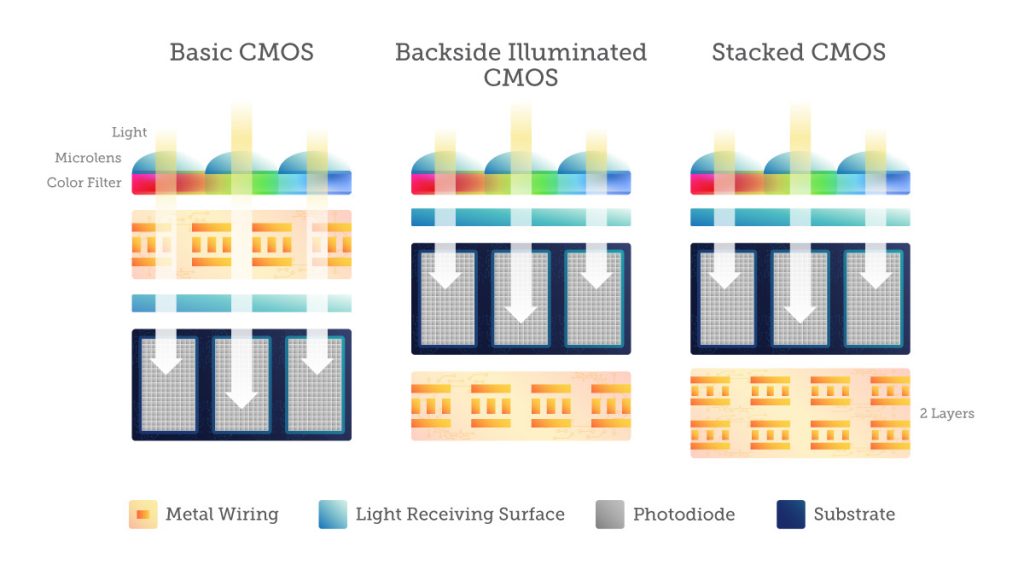
A BSI sensor also has larger angular response, which gives lens designers more creative freedom, and perhaps faster readout speeds. Photodiodes for converting light into electrical signals and pixel transistors for regulating the signals are placed next to one another on the same layer within the pixel chip. To produce great image quality with wide dynamic range, saturation signal level must be increased within form-factor limits.
Crosstalk between adjacent pixels can result in noise, dark current, and color blending, which is a new issue brought about by this innovation. Backside-thinned wafers are more fragile. Even if these issues might be resolved by enhancing the manufacturing processes, doing so reduces yields and increased costs. Despite these drawbacks, early BSI sensors were employed in specialized applications where their superior low-light performance was crucial. Early uses included industrial sensors, security cameras, microscope cameras and astronomy systems.
And this was only the start. While BSI imaging offered specific imaging benefits, it also had far-reaching effects on chip architecture. Chip designers can now think outside of a single plane thanks to BSI technology. The back-illuminated pixel imaging chip of a stacked CMOS image sensor sits on top of a layer (or tiers) of processing chips, allowing for a more vertical construction. What else could you put beneath the photosensitive layer, now that it’s on top? And how far could you go in terms of extra functionality?
Turning Chip Design on Its Head: From BSI to Stacks
Over time, designers have been adding more functionality to conventional CMOS chips to increase both performance and versatility of their imaging sensors—timing generation, power biasing, ADC and control features, and more. In some cases, including those where imagers must capture and digitize hundreds if not thousands of images per second, this has meant the pixel array is not even the dominant piece of real estate on a given die!
This creates some compromises for the chip as a conventional design requires it all to be on the same plane. To get the same imaging performance with the added features, you may need a larger, harder-to-manufacture, and more power-hungry chip in your imaging system. Or you need to decrease the size of the image sensor on the chip, potentially hindering performance.
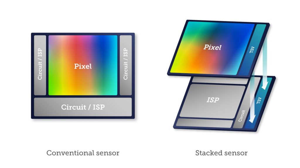
Engineers immediately recognized that this stacking could allow for smaller devices with similar functionality and lower fabrication costs. Sensor designers can separate detection and processing onto their own layers, allowing them to independently optimize detection and imaging processing. They can add circuitry beneath the pixels to achieve lower skews, even across large imaging chips.
It was also clear that 3D stacked sensors could bring more functionality to the CMOS image sensors and remain cost-effective in a way that would never be possible with a single-plane layout. It would be possible to design chip families for more specific applications and industries, providing customers with maximum differentiation.
Stacking for Speed
One of the first examples of stacked sensor performance was seen in the professional camera space, where stacking integral memory, the signal processing circuit, and the image processing engine beneath the pixel layer enabled previously unheard-of frame rates and readout speeds in a full-frame camera.
This was just the beginning. Almost any industry could benefit from faster cameras. At the extremes, high-speed imaging is a key technology to study phenomena such as micromechanics, explosives, plasma formation, and laser ablation. Typically, high burst imagers are CCD sensors, which have very high power requirements, and are constrained by compromises from the in-pixel memory that limit the frames captured to 100. A CMOS solution has advantages, like the ability to embed functions like ADC or compressive sensing. With conventional CMOS sensors, this kind of burst performance was also very difficult, with small pixel fill rates, limited scalability, and frame captures typically in the dozens.
In 2018, researchers at Grenoble University brought 3D stacked sensor design to the problem, creating a CMOS burst imaging sensor that could capture data at a rate of 5 million frames per second. This was accomplished by adding memory to a bottom tier below the imager, capable of capturing hundreds of images at a time, with their research pointing the way to RAM-based solutions that could capture thousands!
Neural Network on a Chip?
The ability to add new features to a CMOS imager has transformed sensor function so that it has become much more than a device for capturing images. There is potential for implementing intelligent functions into the chip, from noise reduction to complete image processing algorithms. This could enable more compact, power-efficient chips for applications that really need it, such as 3D and time-of-flight imaging, event-driven sensing, augmented reality, and even artificial intelligence.
Large arrays of computational units directly connected to pixels could pave the way to on-chip convolutional neural networks and deep learning engines. Energy consumption is an urgent problem in this space, and moving computation to the chip itself has benefits. For one, pixel data can be processed closer to where it is generated, reducing data transmission energy, which can dominate overall energy consumption. Second, the pixel data that originates as analog data can be processed, skipping the energy-intensive analog-to-digital conversion required for external data processing, which often dominates conventional hardware overhead as well as downstream computation and memory energy consumption.
This idea is not new at all. Thirty years ago, a group of researchers at Seville University (the same group that later became part of Teledyne Imaging’s Machine Vision Sensors team), was actively designing CMOS Vision Sensors (CVISs) where each photodiode was surrounded by a hundred transistors. These implemented storage and spatiotemporal filtering (convolution masks, diffusion process etc.) enabling the extraction of features such as edges, corners or interest points, blobs or region of interest, ridges etc. right in the same plane as the pixel array. At the time, lacking stacked sensor technology, this was done at the expense of large pixel pitches, leading to low-resolution devices. However, now the situation has drastically changed.
Researchers still consider this concept of sensor-processors “an exciting playground for exploring a diverse range of trade-offs.” They discussed one example of a CMOS CIS capable of executing an object detection DNN directly, the data volume that has to be transmitted out of the sensor is simply a few Bytes (object location and label), instead of a 6 MB/1080p image. But different power and performance limitations become crucial. For example, getting a performance advantage from on-chip processing, you may need newer, more advanced process nodes. And the power density of a stacked chip with many computational units could generate more heat than a conventional chip, introducing thermal-induced noise that requires more processing downstream.
3D-Stacked Image Sensor Architectures Can Shape the Future
This new approach to chip design and demonstrations of successful commercial technologies is now generating large levels of interest. In-pixel circuitry and connections are offering increased fill factor (responsivity), multiple memory nodes, reduces motion artifacts, and new more efficient HDR techniques.
3D-stacked CMOS image sensors are driving a revolution in many time-resolved, next-generation application domains including LiDAR, biomedical, and quantum technologies, since they hold great promise for much higher fill factor and much more functionality per pixel.
The advances in the last few years have been considerable, and it’s clear that stacked CMOS is just getting started, and customized chips for demanding applications will be a leading source of competitive advantage across multiple industries.
 CMOS TDI: A Game Changer in High-Fidelity Imaging
  Keeping up with CMOS Sensor Design