

AI-Powered Optical Inspection Can Find Nanoscale PCB Defects
Sapera Software Suite makes it easier to use machine learning in AOI with surprisingly few samples
The size and competitiveness of the mobile phone industry has driven investment and innovation in many industries, from imaging to software to even metallurgy. Few industries have been as affected as the semiconductor market, where demand for higher performance in smaller packages has been unrelenting for few decades. Last month Apple released its latest iPhones, some powered by its new A17 Bionic chips, built on TSMC’s new 3nm manufacturing process. Apple is reportedly buying up everything that TSMC can manage to make. These chips are reportedly smaller, faster, cooler, more power-efficient than their 5nm predecessors. According to Apple, each chip features 19 billion transistors, some so small that their elements are only 12 silicon atoms wide.
The same pressures extend to printed circuit board manufacturing: Apple will reportedly switch to using resin coated copper (RCC) foil for their new PCB material, allowing the company to makes them even thinner. This will be challenging for manufacturers, as RCC foil is very delicate, with researchers publishing in IEEE that its especially vulnerable to heat and pressure in the laminating process.
It’s not enough to be innovative – you must return a profit. New reporting from The Information describes the favorable terms that Apple has secured to keep its costs down: in return for the huge orders TSMC has to absorb the costs of defective processor dies. So while fabs like TSMC are touting their competitiveness with ways to develop smaller node processes to reduce chip size and lower power consumption, they will have tough challenges on the quality side.
Automated Optical Inspection for PCB Quality Inspection
For many companies, quality control is the major bottleneck in the PCB manufacturing chain, including reliability testing and reworking defective PCBs. Improving the speed and efficacy of quality control can significantly increase the production yield and throughput, reducing manufacturing costs and waste.
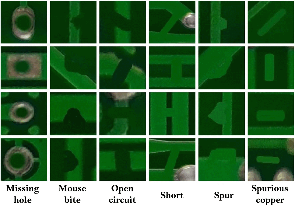
Most PCB manufacturers use automatic optical inspection (AOI) to monitor defects in their printed circuit boards. This delivers strong results when there are defects in the soldering, connections, pads and traces on printed boards.
AOI also proves very useful for the early detection of problems that happen during assembly, such as shorts, open circuits, thinning soldering, scratches on traces and more. In particular, scratches can be “fatal” to a board, changing its electrical properties and causing a total malfunction of the completed product.
AOI has the advantage of being included directly at the end of the PCB production line, before lamination and etching, detecting possible defects earlier than other methods. Imaging systems capture high-resolution images, with resolution down to a few microns, and then comparing them to images of a ‘perfect’ model board (also known as the “golden board”) or with an image database of both acceptable and defective samples.
Other than performing tests on the PCB under assembly, the AOI method can monitor the manufacturing process itself. Pick-and-place machines can respond to detected defects in real-time, correcting assembly defects like component misplacement and misalignment.
Moving Past the Conventional toward Artificially Intelligent Imaging
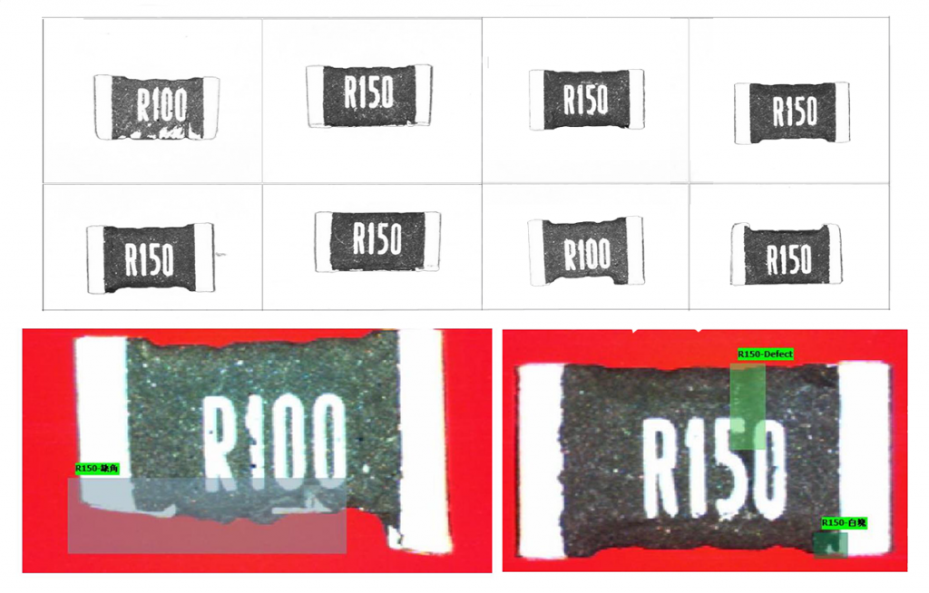
Still, with the demand for smaller, higher-performance parts, the resulting complexities and subtleties in material faults means that traditional manual inspection or rule-based imaging may simply not be up to the task. One semiconductor OEM needed to detect a variety of subtle defects on PCB components, including breakage, abrasion, contamination, fragments, and air bubbles. However, using traditional rule-based image processing was not providing the accuracy they required. They were facing an increase in defective parts that went undetected in their existing process, driving up costs. They needed a new solution.
To overcome these obstacles, the OEM decided to explore machine learning to meet their accuracy requirements for detecting defects on PCBs and their components. They chose Teledyne’s Sapera AI inspection software suite. The Sapera AI software allowed them to expand on their rule-based algorithms with AI functions within their AOI machine. The Sapera AI software turned out to be an ideal solution for the OEM, allowing them to use much of their existing system while providing more accurate detection of the subtle defects that other methods would miss, including breakage, abrasion, contamination, and fragments
Using Sapera AI, the OEM was able to achieve 98% accuracy in continual classification with 12-14 ms speed for 200 images and 100% accuracy with 453 good+ 11 bad images. Additionally, they were able to achieve 99.62% accuracy with 259 images and 20ms speed for object detection when looking for multiple defects on a part image at the same time.
This is representative of the huge improvements that have been made in machine learning over the past few years. While an AI system typically needed to be trained from scratch, requiring hundreds or even thousands of image samples. However, today’s deep learning software is often pre-trained, so users may only need tens of additional samples to adapt the system to their specific application.
The result was a production line that could accurately detect subtle defects on printed circuit boards without the need for labor intensive manual inspection. The AI functions provided a reliable and consistent alternative to traditional rule-based image processing which had previously been unreliable in detecting subtle defects.
Overall, the OEM experienced significant improvements in both accuracy and speed of defect detection on PCBs because of Teledyne’s Sapera AI software, allowing them to reduce fallout while providing higher quality products that met their specifications.
Getting Ready for 2030
Today, the industry is still recovering from the worldwide semiconductor shortage that began in 2021. While analysts like McKinsey predict that nearly 70 percent of growth in semiconductors over the next decade will be driven by just three industries: automotive, computation and data storage, and wireless communications, these industries are still playing catch-up from missed product launches, delayed rollouts, higher prices, and increased expectations. The pressure is on.
Machine learning and AI-informed software systems can quickly improve speed and accuracy in their biggest bottleneck: quality control. Instead of a problem, companies can turn quality control into a competitive advantage, improving speed and lowering costs while building trust in a very tight-knit industry.
Better products may be just the beginning. Semiconductor companies are already leaders in generating and analyzing data, but the insights that machine learning and AI offer may also enhance the other parts of each company’s operations. Predictive maintenance and yield, R&D investment, and even market strategies and product optimization may benefit from bringing more data and better learning.
 The Future of CMOS is Stacked
  Advances in AI for Industrial Inspection